
Technical Capability Overview
The table below summarizes our general manufacturing range. For any values beyond the standard window, our engineering team will evaluate your design and confirm feasibility.
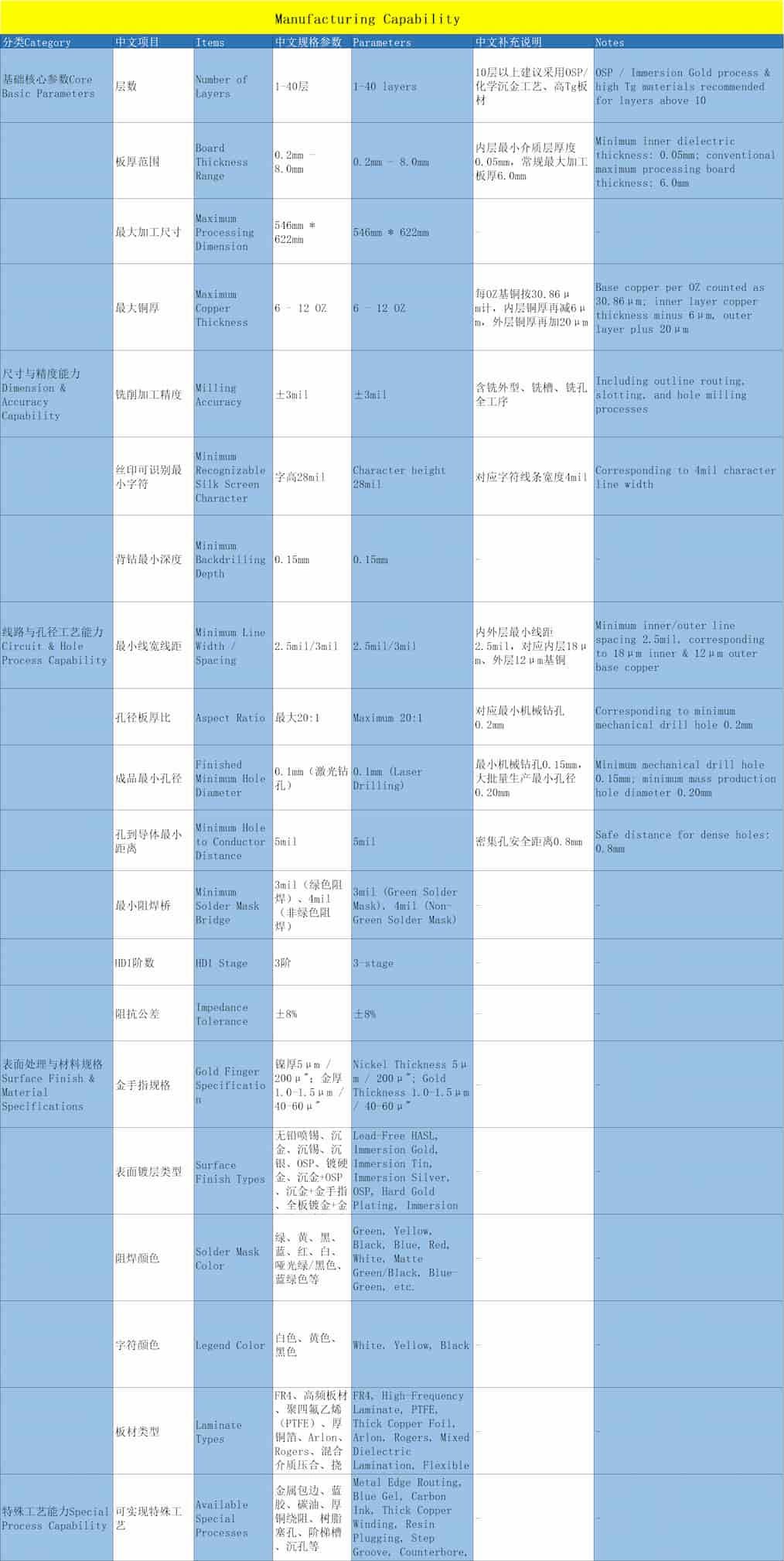
Main Highlights
- Layer count: 1–40 layers (HDI and special stack-ups upon request).
- Min. trace/space and via sizes follow strict IPC Class 2/3 standards.
- Multiple surface finishes: HASL, Lead-free HASL, ENIG, OSP, etc.
- Support for impedance control, thick copper, and special materials.
Standard Lead Time
Time-to-market is critical for R&D teams and small-to-medium batch production. The lead-time table below is a general reference for expedited samples and small batch orders.
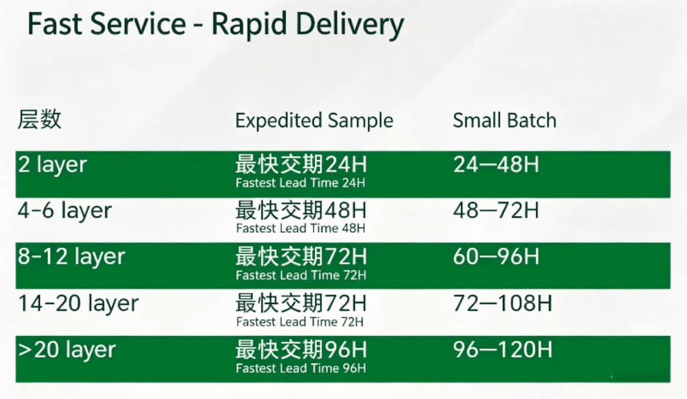
Typical Lead-Time Reference
- Expedited prototypes for standard FR-4 PCBs starting from 24–48 hours.
- Small batches commonly shipped within 3–7 working days depending on complexity.
- HDI and special material PCBs may require additional time after engineering review.
Need to Confirm a Specific Capability?
For detailed capability questions or to confirm if your design is within our process window, please send your Gerber files and key requirements (layers, thickness, copper, finish) to our engineering team.
Email: sales@yostarpcb.com or emily@yudapcb.com