
Product Categories
Yuda Electronic Technology specializes in multilayer PCBs, HDI PCBs with microvias, high-frequency RF PCBs, rigid-flex PCBs, blind & buried via PCBs, impedance-controlled boards and hybrid-lamination PCB solutions. Below is an overview of our main product types.
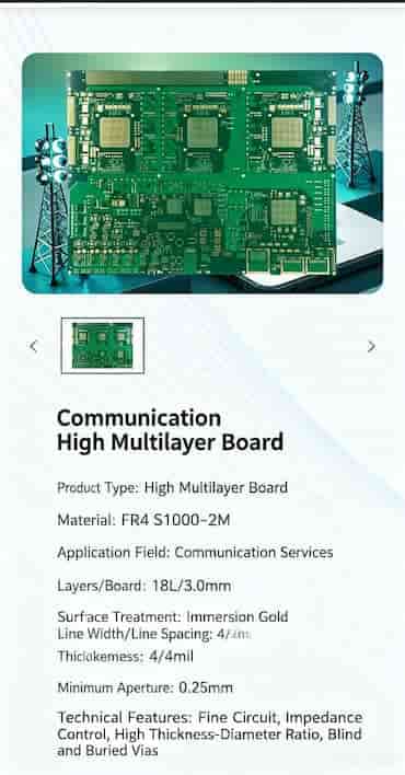
Multilayer PCB
Standard FR-4 multilayer PCBs from 4 to 40 layers for industrial control, telecom and power electronics.
- FR-4 base material, Tg135 / Tg170 options.
- Layer count: 4–40 layers with customized stack-up.
- Board thickness: 0.6–2.0 mm typical, other thickness on request.
- Surface finish: HASL, Lead-free HASL, ENIG, OSP.
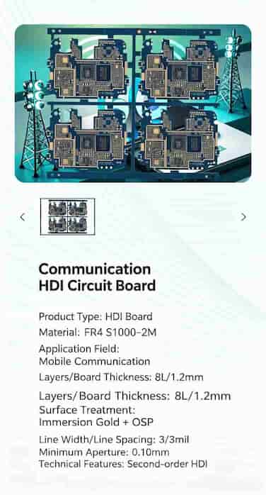
HDI PCB
High Density Interconnect PCBs with microvias, ideal for fine-pitch BGA and compact portable devices.
- HDI structures: 1+N+1, 2+N+2, up to 3+N+3 (case by case).
- Laser microvias, staggered or stacked via options.
- Via-in-pad for high-density BGA layouts.
- Impedance control and high-speed routing support.
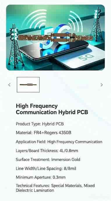
High-Frequency PCB
RF and microwave PCBs using Rogers and other low-loss materials for high-frequency signal integrity.
- Materials: Rogers, PTFE and hybrid FR-4 combinations.
- Stable dielectric constant and low insertion loss.
- Suitable for 5G, base station and RF front-end modules.
- Impedance-controlled lines with tight tolerance.
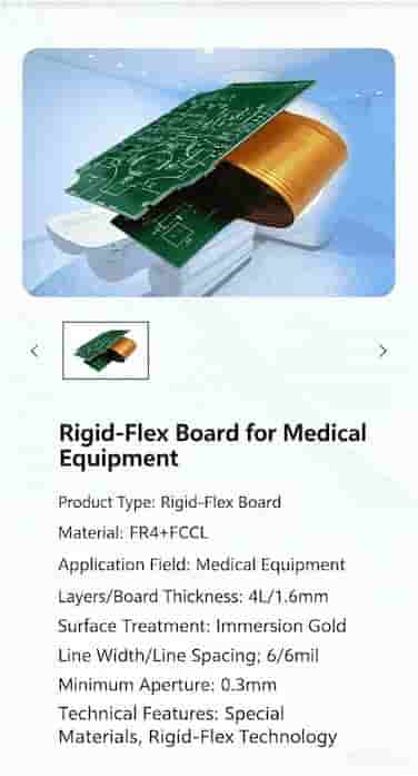
Rigid-Flex PCB
Rigid-flex PCBs for space-constrained and high-reliability applications such as medical, wearable and aerospace devices.
- Polyimide (PI) flex materials for dynamic bending.
- Optimized for 3D assembly and miniaturization.
- Custom stack-ups and coverlay window designs.
- Improved reliability compared to cable assemblies.
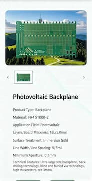
Blind & Buried Via PCB
Advanced via structures enabling high-density interconnects without compromising signal integrity.
- Blind vias and buried vias between selected layer pairs.
- Stacked or staggered microvia configurations.
- Ideal for complex multi-layer and dense BGA designs.
- Options for via filling and copper capping.
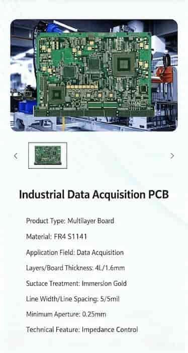
Impedance-Controlled PCB
Multilayer PCBs with controlled impedance for high-speed digital and RF designs.
- Single-ended and differential impedance control.
- Coordinated stack-up design and trace geometry tuning.
- Impedance coupons and test reports available.
- Support for HDMI, USB, PCIe and RF circuits.
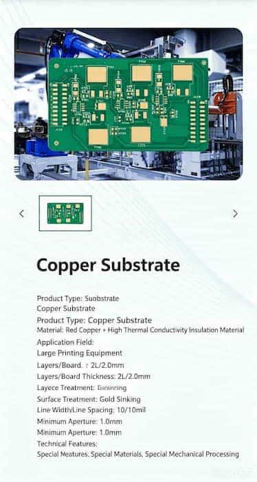
Hybrid Lamination PCB
Hybrid PCBs combining FR-4, high-frequency materials or metal cores to balance cost, performance and thermal management.
- Mixed dielectric stack-ups (e.g. FR-4 + Rogers).
- Local high-frequency zones with low-loss materials.
- Metal-core and thick copper options for power boards.
- Custom designs for special mechanical or electrical needs.